The Delay Circuit
The circuit
 |
The 74HC123 monostable is triggered by a pulse from the GPS, and creates a 5V pulse of at least 10µS. This is reduced to 4V by the divider formed from the 6K8 and 68K resistors as the upper leg, and the 33K and 100K (via the 220nF cap) as the lower leg.
This is compared in the LM311 to the 4V created on pin 2 by the 5K6 and 22K resistors.
If the comparison is successful, the microprocessor is interrupted via the RB0 input. However, success is not guaranteed. If the voltage at pin 3 of the LM311 is zero before the pulse arrives, the 1nF capacitor has to charge to 4V and theoretically this takes an infinite time.
It follows that for successful firing, the voltage at pin 3 should be positive but less than 4V. This voltage is provided from the microprocessor via RA2. RA2 can act as a voltage source, or as a logic source. Both modes are used by the system.
|
Setup mode
When the system is trying to synchronise the OCXO to the GPS, it is desirable that there is a fixed delay between the GPS creating a 1ppS pulse and the triggering of RB0. To achieve this, RA2 operates as a voltage reference, providing a fixed bias of approximately 2V to pin 3 of the LM311. This 2V is added to the waveform of any incoming pulse, guaranteeing the LM311 will pulse RB0.
Delay mode
Once the approximate arrival time of the GPS is known, the processor can vary the voltage on pin 3 of the LM311. This changes the delay between the GPS pulse triggering the monostable and pin 3 reaching 4V. If the voltage is near 4V, only a small extra charge of the 1nF capacitor is required to reach 4V. However, if the voltage is close to zero, more charge is required, and it will take longer to reach 4V. If the software were to try and set an appropriate voltage for a particular delay, the relationship is an addition of two exponential curves and is a complex calculation. The solution lies in providing a fixed charge, then allowing the charge to leak away via the 100K resistor. The rate of discharge is also an exponential curve but the two curves are now in the opposite direction. Because the two curves are based on the same voltage, the delay of the GPS pulse is a linear relationship to the time when the discharge starts.
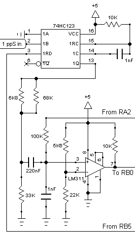
This is a simulation of what happens at pin 3:
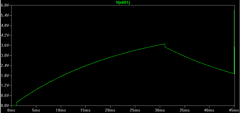
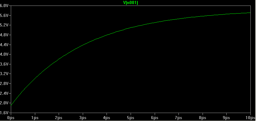
Note the spike at the 45ms mark. It is in fact an exponential curve - with an expanded time scale it looks like this:
The component values in the circuit are chosen so that varying the start of discharge 100µS (that's the time between TMR2 interrupts) varies the pulse delay by approximately 20nS. In the software, the start of discharge time is controlled by an 8-bit variable (0-255), which allows the pulse delay to vary by about 5µS.
Why it works
There are two RC networks determining the time when Pin 3 of the LM311 reaches 4V. When RA2 goes high, the 1nF and 220nF capacitors charge up from current flowing through the 100K resistor. The 74HC123 has an active low so the charge for the 220nF capacitor also flows through the 6K6, 68K and 33K resistors to earth. This is why the trace of the charge/discharge shows a little jump at the start of charging and a little drop at the end - it is the ratio of the 100K resistor, and the other 3 resistors acting in parallel. The time constant of this RC network is around 25mS. When RA2 goes low, the capacitors start to discharge via the same paths.
When the 74HC123 receives a 1pps pulse from the GPS unit, its pin 13 goes to 5V for a period set by the 10K and 1nF components of about 10uS. The 1nF capacitor on pin 3 of the LM311 is charged further (it has the residual charge from the charge/discharge cycle) by this pulse via the 6K6 and 68K resistors. The 220nF capacitor has no time to change its charge, so acts as a constant voltage increment to the voltage applied by the 6K8+68K resistors, and the 33K+100K resistors act as a voltage divider. Effectively the 1nF capacitor and the 6K8+68K resistors act as an RC network with a time constant of 10µS.
It is the big difference between the two RC constants that allows the microprocessor to precisely change the delay in nanoseconds with an event (the discharge initiated by RA2) measured in many microseconds.
Calibration
The microprocessor needs an estimate of how long to charge the network via the 100K resistor. It does this during startup by disabling the 74HC123 via the RB5/1RD link which blocks the GPS pulse. It then applies 5V to the 100K resistor and measures the time it takes for the LM311 to trigger RB0. This time can then be used to calculate how far in advance of a GPS pulse the capacitor should be charged. The time is checked to see if it is within limits and the program aborts if it fails the test. When in run mode, the charge is continually measured and the charge times refined, to compensate for any temperature variation.
Also needed is the delay change for one increment of the 8-bit variable controlling the start of discharge. This is computed by applying control volts known to cause the OCXO to deviate by plus and minus 1 part in 108, then using the delay circuit to track the GPS pulses for a few seconds and noting the change in the 8-bit variable in that time.
Software Control
Control of charging
Charging of the delay circuit is initiated by raising pin RA2 of the processor. This is done in the TMR2 interrupt, when the 1 second counters are at the same value as the variable PreStart. PreStart is set by the mainline. At the same time, the TMR2 routine clears and starts Timer 1 (16-bit), and sets a flag (ChgFlag) to let the RB0 routine know why it was interrupted.
Once RA2 is raised, charging continues until the capacitor is at 4 volt, and this triggers the RB0 interrupt. The RB0 interrupt tests the flag set by the TMR2 routine, and because the flag is set the routine clears the flag, drops the RA2 pin, and stops Timer 1.
Timer 1 measures how long it takes to charge the capacitor to 4 volt. The timer increments every 3.2µS. It is clocked by the instruction clock (400nS) divided by 8 in a prescaler. The mainline calculates using a timing increment of 100µS, that being the interval between TMR2 interrupts. To convert from Timer 1 increments to approximately 100µS increments can be achieved dividing by 32 (giving 102.4µS increments which is close enough). A slightly different approach is used - instead of dividing each Timer 1 value, the TMR2 routine accumulates 8 values in a 3 byte accumulator and then discards the least significant byte. Mathematically it is equivalent to 8/256, or 32 as desired. It has the advantage of averaging the value over 8 samples. The accumulated 2 bytes are transferred to ChgLen every 8 seconds for use by the mainline in calculating the next value of PreStart. Timer 1 is only set to zero by the TMR2 routine at the start of a charge cycle, so when there is no charge cycle the last value of Timer 1 is repeatedly read, giving a valid result.
The reason for continually deriving ChgLen is that the capacitors are ceramic and show some temperature dependancy. A hardware solution is to use NP0 capacitors, but this technique compensates for the change, so allowing the use of cheap components. The author considered using a temperature dependant resistor in the charge circuit to allow temperature monitoring, but this was not done.
Tracking the GPS
When a GPS pulse, after delay, causes the RB0 interrupt, the value of TMR2 is compared with an expected value. During setup, the difference in value can vary from -100 to +100 although this is unlikely as it indicates huge frequency errors. The measurement is in instruction cycles of 400nS, so a difference of 100 is 40µS in one second, or 4 parts in 105. It is unlikely to find a crystal with that error A difference other than zero indicates the oscillator is slow or fast. A value of zero, however, is ambiguous. Consider the situation where a GPS pulse arrives half way through an instruction cycle. If the subsequent pulse arrives somewhere in the cycle 2,500,000 instructions later, it will give a value of zero. It could arrive early in the 400nS period or later depending on if the oscillator is slow or fast, but that will not be noticed because it is less than the granularity using just the instruction periods. During most of setup, this is not an issue as the oscillator is running sufficiently fast or slow to eventually cause a +1 or a -1 and by counting the number of zero results between them, a frequency error can be calculated.
However, once the oscillator is thought to be locked, it is desirable to know the relationship to better than 400nS. The solution is to vary the pulse delay between pulses to make the time between pulse detection longer or shorter. The aim is to receive values of zero or -1. If the delay is not changed, a -1 indicates the oscillator is running fast, but that might mean 10.000000000001MHz instead of exactly 10MHz. If the detector had been altered so the next pulse is detected a little later, the result would have been zero. In practice, the GPS can be tracked by continually changing the delay. If the result is -1 starting the charging earlier will cause the pulse to be detected later. If the result was zero, start charging later to detect the pulse earlier. That way, the pulse detection time ends up within a few nanoseconds of the transition from one instruction to the next.
The amount of delay applied can be varied over 256 steps, controlled by a 1 byte variable (PreVal). The software aims to keep PreVal at the middle of the range (128 or hex 80), and at the end of each period makes adjustments to the OCXO control voltage to achieve that. However, during a run period the OCXO control voltage is not varied to follow the GPS, so the software has to vary the delay to center the pulse detection on the instruction transition. Assuming the GPS is correct, the difference between PreVal and 128 is the frequency error. In practice the GPS will deviate in the short term so the deviations have to be averaged for calculation.