| Back |
Hardware Design |
This section discusses why the design is the way it is, and how it may be modified
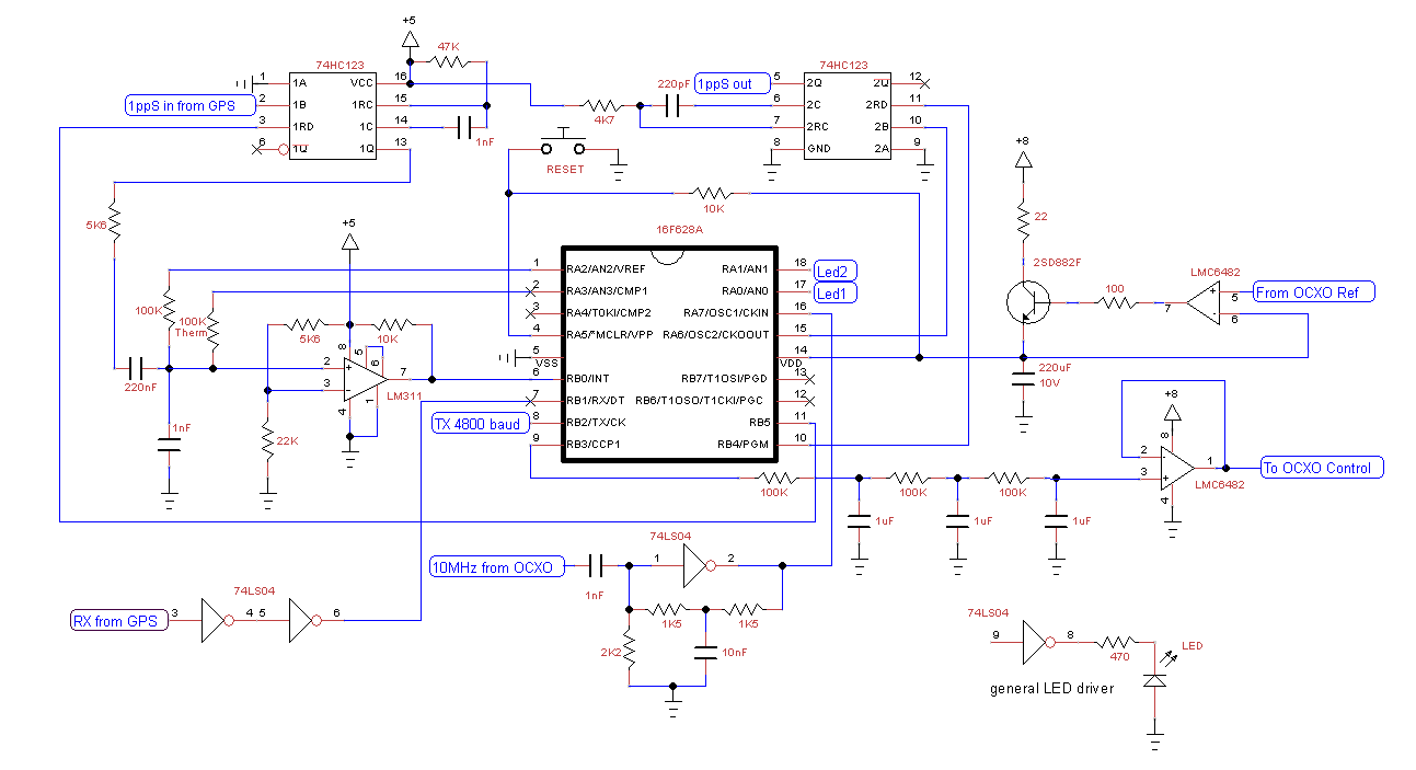
The 1ppS first triggers a monostable to produce a pulse about 20µS duration. It was not clear from the GPS module documentation what duration 1ppS it produces, and also (I later found out) it is only a 3.3V output and the optimum voltage is the same as that provided as the -ve input to the comparator. This was set to 4V by the 5K6 and 22K divider so a greater voltage was desirable. The monostable also has an enable pin, so the processor can block pulses if required. The pulse charges the 220nF and 1nF capacitors, which act as a voltage divider, via the 5K6 resistor. Because of the big difference in value, over 99% of the pulse voltage is applied to the 1nF capacitor. At the time the pulse arrives, the junction of the 220nF and 1nF has a residual voltage provided by the processor either by RA2 or RA3 via its associated 100K resistor. The magnitude of the voltage determines the delay between the pulse being created by the monostable and being detected by the comparator. The comparator then causes a processor interrupt via RB1.
The processor has two modes of operation. Before the OCXO frequency is close to the desired value, RA2 is connected to the internal voltage reference to provide just over 2V and RA3 is set as a high impedence input. This permanent bias to the junction of the two capacitors ensures the comparator is triggered at any time a GPS pulse arrives. Once the OCXO is roughly adjusted to the correct frequency, the arrival time of the 1ppS becomes predictable within a window of a few hundred nS. At this stage the junction voltage is made variable. This is achieved by charging the junction to 4V from RA3 via a thermistor while RA2 is configured as input. Charging is stopped by the RB1 interrupt handler which sets both RA2 and RA3 as inputs. The charge is held for a few milliseconds then at a predetermined time before the expected arrival time of the 1ppS RA2 is set to output low which discharges the capacitors via the 100K resistor.
This may seem overly complex. It is done this way because the start of discharge has a reasonably linear relationship with the 1ppS detection delay. Varying the start of discharge time by 100µS varies the delay by nanoseconds (about 16nS in the circuit as built). In theory the relationship is linear if the comparator voltage is the same as the voltage pulse provided by the monostable. In an earlier circuit this was attempted but using a 5V pulse seems to make no practical difference. In software, the start of charge and the start of discharge are handled by the TMR2 interrupt handler. The charge reaching 4V and the pulse reaching 4V are handled by the RB1 interrupt handler.
Because most GPS units are able to run from 3.3V, and the processor is run at 5V to provide the 0-5V control voltage, there is scope for eliminating some hardware. It is quite possible the processor internal comparator is adequate. If so, assuming the GPS pulse is of reasonable duration and the GPS module has an active low, the GPS output could directly supply the resistor/capacitor network. The GPS Vcc can be connected to -ve input to the comparator which is close to optimum. The ability to block 1ppS in the hardware is lost, but this can be implemented in software.
The processor is clocked by the OCXO output via one inverter. The input is biassed into conduction by the filtered feedback from the output. Without the 2K2 resistor to earth, the processor would not run. This may have been due to a lopsided duty cycle. The 2K2 resistor corrects this, with the input measuring around 1V and the output about 2.5V (which may be 50% duty cycle, but as I have no instrumentation this is just an assumption). There are likely to be other ways to derive the processor clock from the OCXO, this just happens to work.
Note the 10MHz from the OCXO is not brought out to a connector. In the picture below the 10MHz is output to strip under the second bottom row of holes, the only connection being the capacitor to the 'LS04. It probably should be terminated but I was not sure how. The strips either side are earthed.
LTspice was used to design the extreme filtering of the PWM to provide the control voltage. It eliminates all PWM and dithering artifacts. The Morion OCXO has a low impedence input so it was necessary to buffer the high impedence of the filter using an op amp. Since building the circuit, it has become clear that the 100K/1µF combination could be replaced with any combination with the same RC constant - e.g. 1K/100µF. The high capacitor values were not considered due to unwarranted concerns about using electolytics with low voltages. The conclusion is that a much lower impedence filter could be created thereby removing the need for the op amp. It would not be able to output the full control range, but that may not be an issue. The Morion, even though it is quite old, requires a voltage around 2V.
The double inverter is used to level shift the GPS serial output from 3.3V to the 5V required by the processor. This was added when it was found the GPS module continued to generate 1ppS signals even though it had lost contact with the satellites. The processor now decodes the $GPRMC and blocks the 1ppS if the signal is not valid.
As there were spare inverters, two were utilised to buffer the processor output to drive the LEDs. This is probably unnecessary as the processor is quite capable of driving the LEDs. As it is, they should be wired so that a high from the processor turns on the LED. This is because the 'LS04 can sink more current than it can source, and also is more logical.
The Morion has a 5V reference so it was used to control the Vcc which in turn provides the voltage for the PWM. This may or may not be better than using the output of a standard 5V regulator such as a 7805. When the circuit was first constructed there was no thought of using temperature compensation. Now that temperature compensation can be implemented, any variation in supply voltage due to ambient temperature variations can be corrected perhaps removing constraints on the supply.
This was provided as an afterthought. The time constant is very short, if the facility is required a constructor should choose appropriate values for their own application. Due to software constraints it was not considered feasible to generate 1ppS aligned with the input 1ppS. It is generated about 150µS later. Because the processor is locked to the OCXO, the 1ppS should have negligable jitter, certainly less than that available from the GPS module.
This is a prototype designed on paper and has had only a few modifications since it was built. It could do with a redesign based on what has been learned since. Such is the power of hindsight. It is presented 'as is' more for the value of the ideas than for its actual implementation.
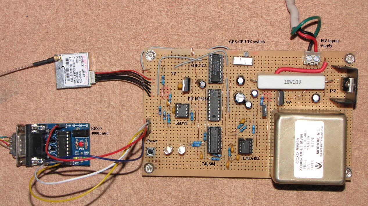
The layout is quite haphazard, the ICs are all socketed because some wire wrap sockets were in the parts box. The long pins under the board were used to mount some component but most are visible. There is a switch that selects either the TX output of the processor or the TX output of the GPS to be sent via the serial interface to a monitoring PC. The MC78T12 regulator can be seen on the right with a small heatsink. The 1 ohm 10 W resistor is between the laptop supply and the regulator, partly to limit inrush current, partly to distribute the heat load. The power supply to the OCXO is done in heavy gauge wiring on the underside. There is also a heavy gauge wire soldered across all the conductive strips of the Veroboard to act as an earth plane, with individual earths connected to it via the copper strips.